nobcha23の日記

PICマイコンやArduinoを使う電子回路遊びを紹介します

R909-PANEL基板にオシロ機能を移植 I have incorpolated the oscilloscope function on the R909-PANEL PCB

YoutubeにポストされているOLED仕様の簡単オシロをR909-Panel基板に改造移植してみました。アイデアにあふれた面白い試作品を紹介された作者ラジオペンチさんに感謝します。

youtu.be


YOUTUBEで同じような画面の試作がいくつか紹介されていました。オリジナルはどれかなのか、手繰っていくとラジオペンチさんのブログにたどり着きました。

There are so many videos to try OLED oscillo scope on YOUTUBE. I found that the original was mostly Japanese site of http://radiopench.blog96.fc2.com. I'm appreciated the blog and I tried to convert the sketch onto my R909-PANEL PCB.
Thanks much for providing cool device.


ラジオペンチ モノいじりが好きなおじさんの探究日誌
私のOLEDオシロを実際に作った人のYouTubeの動画を調べてみた


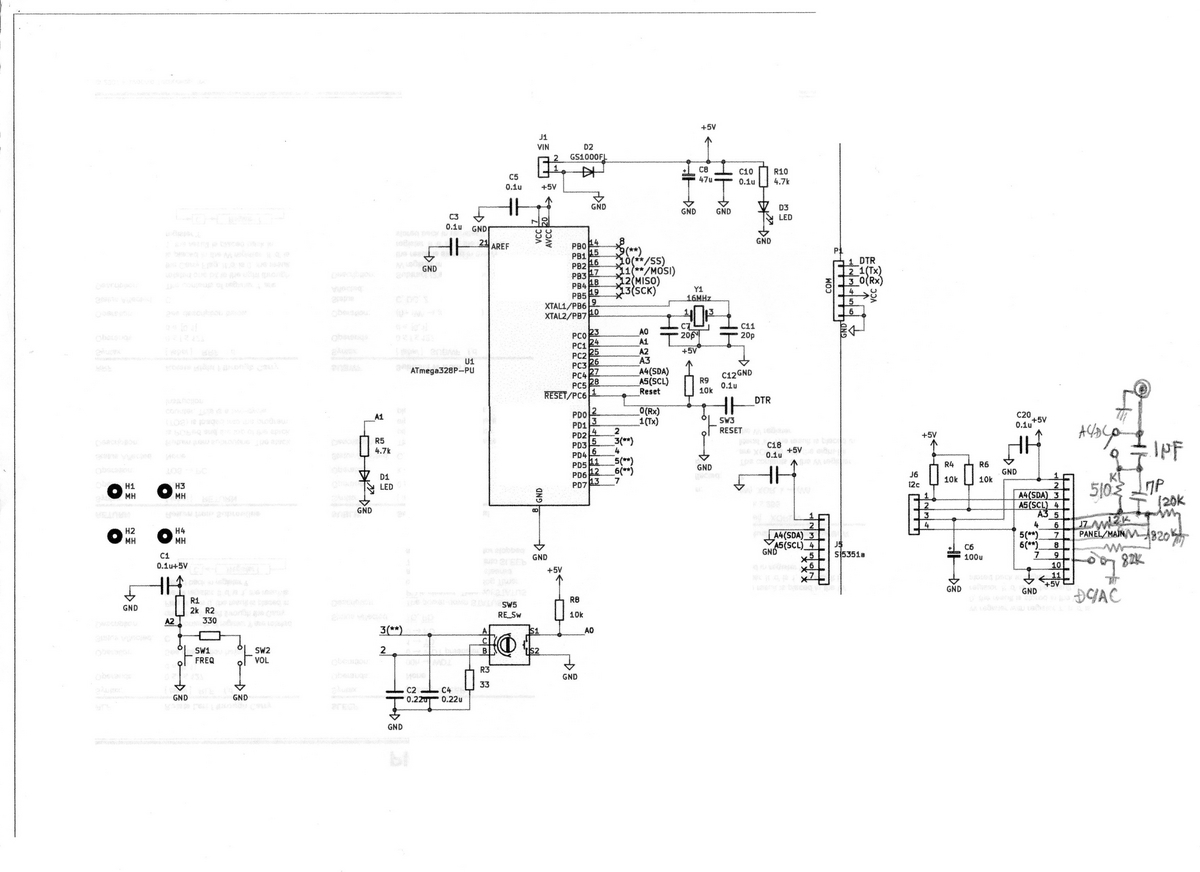
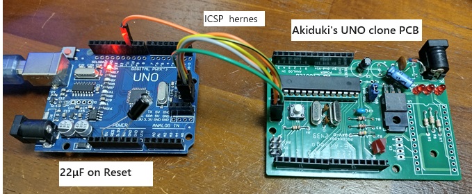
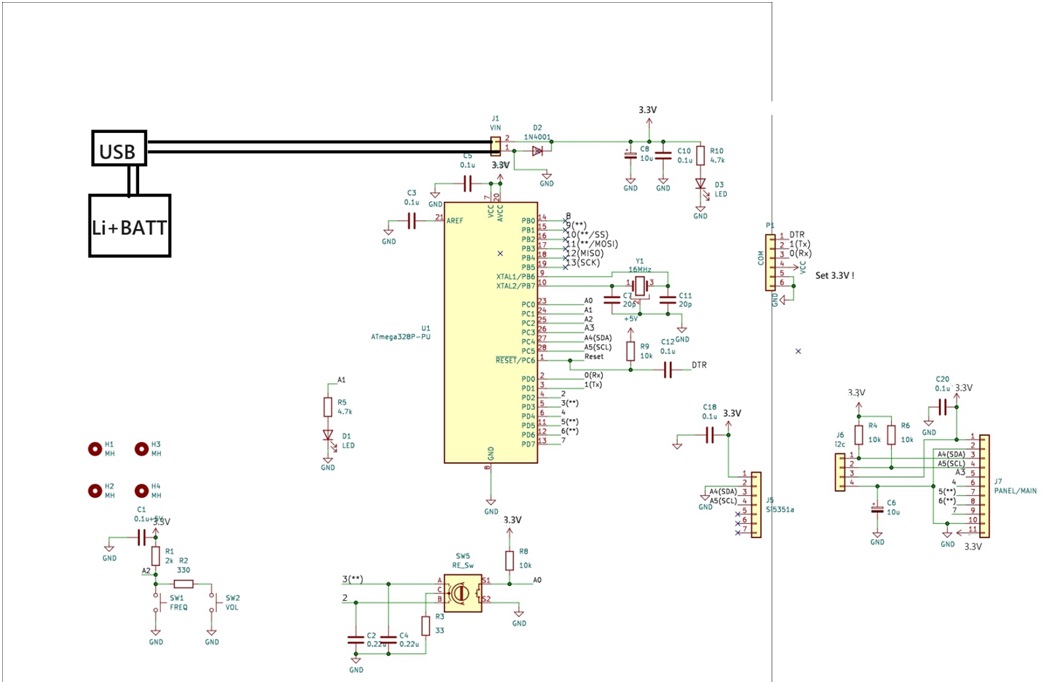
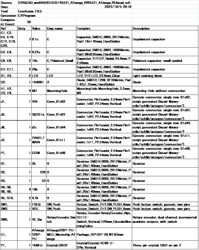
移植先のR909-PANEL基板ですが、Si4732やSi5351aモジュールを制御して受信機を作るために設計したものです。基板はArduinoローダ入りATmega328PとロータリーエンコーダーとOLED表示モジュールからなっています。

入力回路部分はさておいて、まずスケッチがうまく移植できるか検討しました。ポートの変更、スイッチ機能を変更します。SELECTスイッチ機能はロータリーエンコーダープッシュスイッチを利用し、パラメーターの増減はロータリーエンコーダーで行いました。

R909-PANEL PCB is designed for the airband radio control. It is composed with ATmega328P with loader, The rotary encoder, and OLED dsiplay. To convert means to divert the rotary encoder for the switches. The rotary encoder push switch is acting the select and the rotary encoder changes the parameters.

外観
オシロ画面
回路図

http://chitose6thplant.web.fc2.com/AB/R909/20240220_OLEDoscilloScope.pdfスケッチ


The improved version has come from the other bloger, and I would like to follow and also install it in the case later.


Arduinoオシロスコープharahore.g2.xrea.com

http://radiopench.blog96.fc2.com/tb.php/1027-c4e0617a

ケースのパネルを基板で To make the case panel by PCB

J909-DSPのケースですが、Aliexpressで売ってるアルミ引き抜き材のケースとフロント、バックのパネルはプリント基板で作ってみました。


PCB

元々はエアバンド/FM受信機用に作ったのですが、VFOにも使えます。

バッテリー動作のVFOと言うのをケースに入れるに使おうかと思っています。

nobcha23.hatenablog.com

ケースのパネルを基板で To make the case panel by PCB

出来上がった回路を実用的に使うにはケースに入れたいです。
Aliexpressでアルミ引き抜き材ケースが何種類か売られていたので、その中から選び使う事にします。
アルミでも穴あけ加工をきれいにまとめるのは大変なので、今回プリント基板で作ってみることにしました。

PCB


またまたPCBGOGOに依頼しました。事前チェックでまた引っ掛かり、基板を作る前に相談し解決。

プリント基板製造・実装|短納期基板製作|プリント基板実装 - PCBGOGO

ところで、PCBGOGOの2024年春節休み。
www.pcbgogo.jp


To use the DIY radio practically, installing it in the case is preferable.
I found the case made of the aluminum pulling material at Aliexpress.
As drilling the case is hard, I made the front and back panel by PCB.

Many thanks for advising prior to produce the PCB. This time I got some advice from PCBGOGO stuff.

こんな感じで組立てる予定です。
The assembled example is here.

Bought at Aliexpress

Front panel

www.youtube.com

RF信号発生器の回路や基板 There are PCB data of the RF generator on my WEB

ブログで紹介したRF信号発生器の回路や基板やスケッチの情報保管場所です。
I will tell you the WEB site of the RF generator's data as below.

OLED表示RF信号発生器の回路図
The schematic of the RF generator/OLED display

OLED表示RF信号発生器の部品表
The BOM of the RF generator/OLED display

OLED表示RF信号発生器のArduino sketch(UNO仕様のATmega328Pを使用)
The Arduino sketchof the RF generator/OLED display(For ATmega328P as UNO)

プリント基板製造・実装|短納期基板製作|プリント基板実装 - PCBGOGO
PCBGOGOへのユーザー登録
Would you resister to PCBGOGO?

PCBGOGOの2024年春節日程。
2024年春節休み前後の納期につきまして

ーーーーーーーーーーーーーーーーーーー
パネル基板のガーバーデータ提供について
バッテリー動作のRF発生器を作ってみよう I would like to make the battery operated frequency generator - nobcha23の日記

ATmega328PにArduino boot loaderを書いた Write the Arduino boot loader on ATmega328P

Si4732を使うエアバンド受信機を設計デバッグしています。Arduinoデバッグボードではpro miniでしたが、最終形は基板をアルミケースに入れたいので、ATmega328Pを使う予定です。今回チップをECで買い、ブートローダー書き込みしました。

I'm using ATmega328P with Arduino loader the latest RF generator boards to be compact for installing in the case. So I shall make such chips from the bare ATmega328P.

書込みのやり方ですが、ググって出てきた情報でブレッドボードを使って安易にやってみたが、失敗。どうもブレッドボード、ジャンパ線配線では不安定みたいで、環境整備しないといけないと思いました。じっくり腰を入れて探したら、次のWEB内容はまとまりよく、整理されていてわかりやすかったです。参考になりました。感謝します。

I ever referred some kinds of Internet sources and failed some time with the bread board connection. This time I confirmed the writing system according with the below information. Many thanks for providing cool ideas to be put in order.

Arduino ブートローダーを書き込む (AVR)
ht-deko.com


今後また書き込みが必要となった時のため、基板接続、IDE設定をまとめました。記事内容から接続や操作の勘所をメモにしました。接続を間違いないようICSPケーブルを作りました。書き込み機はUNO,被書込み用にはICソケットが付いたUNOコンパチ基板が必要です。秋月電子の150円基板を使いました。必要最小限部品としてはICソケット、16MHz水晶とコンデンサ、ICSPコネクタ、RESET停止用22μF電解コンが必要です。

I'm using UNO for writer, UNO compatible board for written, 22uF, and ICSP cable. The UNO compatible board is composed with IC socket for ATmega328P, 16MHz Xtal, and 22p capacitors.

接続 connection
connection

実際の基板接続

バッテリー動作のRF発生器を作ってみよう  I would like to make the battery operated frequency generator

Si4732を使ったエアバンド受信機を試作していますが、FM放送はチップ単体の機能で受信できました。AMの方に取り掛かりました。調整するにはRF信号源が欲しいと、パネル部(Arduino+Si5351a+OLED+SWs)だけ利用したRF信号発生器をまとめています。
To debug the 4732 RX, I shall need the frequency generator. I assembled that diverting the panel PCB of the 4732 RX. I'm referring CesarSound masterpiece on PROJECT HUB. Thanks much.


パネル部基板ですが、PCBGOGOに追加分作ってもらいました。今回は輸送費を下げるためOCSにしました。11月8日入稿、9日事前チェック通過、13日到着です。見た目仕上がり満足です。
I asked to produce the PCB for PCBGOGO. I sent the data on 8th Nov, got checked on 9th, and PCB arrived on 13th via OCS.

パネル部PCB

今回作るRF発生器では実験時の電源供給やりやすいよう電池動作にします。Arduino入りATmega328Pが、Si5351aモジュールの周波数をロータリーエンコーダーで設定、OLEDに表示を出します。USBコネクタが付いたリチウムイオン電池充電制御モジュールを用い、使わなくなったスマフォの電池を利用します。
To utilise this generator, I'm operating this with the battery which is worn out smart phone battery and USB power charging board.

回路図

ATmega328PやSi5351aモジュールを3.3V化する前にとりあえず電源だけ入れてみました。そうすると電池電圧3.9Vででも動くではありませんか。ATmega328Pは3.3Vでも8MHzなら働くし、Si5351aモジュールに使われているLDO電源レギュレータは軽負荷なら10mVしか電圧を食わないので当たり前なのかしれません。
To change for 3.3V operation set up, I connected the current ATmega328P and the Adafruits type Si5351a module and they worked well. However I will let ATmega328P to change 8MHz and 3.3V loader later.

F-Generator

プリント基板製造・実装|短納期基板製作|プリント基板実装 - PCBGOGO


ーーーー基板製造データ提供ーーーー
この回路ですが、当初は簡単にブレッドボードで組んでいたものです。しかし、ロータリーエンコーダーを回すと、実験操作中不安定になり手間かかるのが対策できました。簡単ながら色々と使い道ありと思っています。古い受信機などの局発デジタル化などにも使えそうかと思います。
ところで、基板製造データを提供する条件ですが、このリンク経由で
プリント基板製造・実装|短納期基板製作|プリント基板実装 - PCBGOGO
PCBGOGOへのユーザー登録をお願いします。取得したIDとメールアドレスをコメント欄か、メールにて連絡いただくと、返信で製造データ、回路図、BOMなどをお知らせします。(コメント欄は公開しません)
IDを今回初めて取得していただいた方には初回注文が送料込み1ドル(ただし振込手数料必要)になる特典が付きます。
また、とりあえず実験で基板を試してみたい方には郵送料手数料200円(Paypalかアマゾンギフト、国外送付は別途相談)で試作基板一枚を定形郵便でお送りします。その際はID,メールアドレス、住所をお知らせください。

PANEL_PCB
BOM

PCBGOGOの2024年春節日程。
www.pcbgogo.jp

The tiny Arduino controled 5351a VFO Si5351aを用いたArduino制御のVFO

I'm designing Si4732 receiver with Si5351a controled by Arduino. Within this there is panel portion PCB of containing ATmega328P, and switches. So I can divert this for VFO.
Si4732Siと5351a局発のコンバーターを組み合わせた受信機を設計中です。その一部分としてコンパクトなパネル部基板を起こしました。

There are ATmega328P, OLED, Si5351a module, and switches on compact circuit board. As the majar function blocks are connecting via i2c, I could easily convert CesarSound's VFO sketch of PROJECT HUB onto this board.
制御はArduinoブートローダー内蔵ATmega328P, OLED SSD1306, Si5351a モジュール, ロータリースイッチとファンクションスイッチ2個です。主要機能モジュールがi2c接続なので、CesarSoundがPROJECT HUBに発表されているVFOのsketchを簡単に移植できました。

動作写真

The signal is pulled out from Si5351a module's SMA output. I inserted ATT between SMA and Si5351a output with cut and jumped.
信号はSi5351a モジュールSMAコネクタ出力から取り出しました。また、SMAコネクタ出口には6dBのATTを入れてあります。

I reedited the sketch for the signal generator. I can use this for testing the receivers.
スケッチを少し書き直し、試験ベンチ用VFOとして使うことにしました。

操作ルールは次。
通常キーステイタス0の時はロータリーエンコーダー回すと指定ステップ周波数単位で受信周波数を増減。
ロータリーエンコーダーのプッシュスイッチでステップ周波数単位を変更選択。
機能キー1を押すと設定周波数バンドを次々と切り替え表示していく。160m>80m>40m>....


PCBGOGO
www.pcbgogo.jp